By Jack Ganssle
December 2014
Rev 1: March 2015 – Added new info about improved Freescale datasheets.
Rev 2: May 2015 – Added link to Low Power Design article.
Rev 3: May 2015 – Added update in section 11 about electron pooling.
Rev 4: March 2016 – Added section 12 about watchdog timers.
Today many of us are building ultra-low power embedded systems that must run for years off a battery. The idea is that these systems are nearly always in a deep sleep mode, waking from time to time to do something before going back to sleep. Many vendors of microcontrollers (MCUs) claim their products can run like this for decades from a coin cell.
These claims are mostly bogus.
This report describes the hardware and firmware issues one must consider when designing very low-power coin-cell products. There are a lot of nuances; even decoupling capacitor selection can hugely influence battery life. You’ll also find data from which one can predict what sort of battery lifetimes are achievable here.
Because the report is very long and covers a number of related subjects, not everyone may need to read the entire thing. Here’s a roadmap so you can get to the sections important for your design efforts:
- Background — Do read this. It gives a bit of information about coin cells, and then shows how the basic assumptions made by MCU vendors are completely off-base. They talk about how long a system can sleep; we care about how much work can be done when it is awake. Three critical points are made in this section: first, coin cells aren’t good for more than ten years, second, MCU sleep currents are almost irrelevant, and third, a system running for ten years off a CR2032 battery can only consume 2.5 uA on average.
- On Typical Specifications — Many MCU vendors make glorious claims about low current consumption and quote astonishing numbers. Dig into the datasheets and it’s not uncommon to find these as “typical” specifications. I investigated what “typical” means. The result: never, ever, use a “typical” specification as design guidance.
- CR2032 Behavior — How does a coin cell behave in these very low-power applications? No one seems to know, so I took a ton of data. The results are surprising and bode ill for long-lived systems. You may find that less than half the battery’s advertised capacity is actually available in a real system.
- Leaks and Drains — The MCU is not the only power consumer on a board. Even the capacitors leak — a lot. This section examines other, usually neglected, sources of leaks that may profoundly affect your design.
- Decoupling, and Using a Capacitor to Boost Vdd — Pick the wrong decoupling capacitor and your system will discharge the battery in a short time. And, given that an ultra-low power system sleeps most of the time and wakes for only milliseconds, can we use a capacitor’s time constant to keep Vdd high enough to power the system during the brief time it is awake? Hint: the answer is no.
- Running Fast to Save Power — The vendors recommend running the MCU as fast as possible to get back to sleep quickly, as the total power consumption will be less than running at a slow clock rate. While that is true, it is naïve. There are other factors to watch out for. This section is important for firmware designers.
- Dropping Vdd to Cut Current and Increase Battery Life — You might get some benefits by reducing Vdd to the MCU, but there are some caveats.
- Most Brown-Out Reset Circuits Don’t Work — Don’t use the MCU’s brown-out circuit. It will not perform as you would expect in most cases. An alternative is presented. Firmware people take note.
- Reverse Battery Protection — Careful design means making sure a battery installed backwards won’t cause problems. Alas, the usual fixes create more problems than they solve.
- UL Coin Cell Requirements — UL is very strict about using coin cells. Here are the rules, and their implications.
- Battery Droop Over Time — With a load on a coin cell the voltage decays for a while… and then, oddly, stops. Figure on another 10% loss of capacity due to droop.
- Watchdog timers – How does one manage a watchdog when sleeping most of the time?
- Summary
- Reviews of tools to profile low-power systems. This isn’t really in this report; this is a link to my web site’s reviews.
Another
great resource on these issues is Low Power Design by CMicrotek.
It covers other important issues about these applications, and is highly recommended.
1 – Background
There’s a sleep current war raging between MCU vendors. Marketing glitz and web pages are the guns; white papers are the ammo, which is being broadsided with increasing frequency. Much of what is claimed is probably true, but more than a little of it is misleading and/or irrelevant.
It’s truly remarkable just how little current is needed to keep a processor alive today. In the deepest sleep modes even some ARM parts claim just 20 nA (nanoamp) of consumption. That’s a mere 0.02 microamp, a number that boggles the mind. In the desktop world CPUs suck over 100 amps while active, so I salute the MCU community for achieving such astonishingly-low figures.
First, some context. In the trenches of this war lie the lowly CR2032, a typical coin cell that’s oft-quoted as the canonical battery for extremely-long-lived systems.
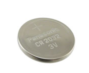
A CR2032 primary cell
A CR2032 has about 225 mAh of capacity (quoted capacities vary a little depending on the vendor), which means it can source one mA for 225 hours. (Note there is some dependency on capacity vs. how fast one discharges the battery). Its nominal voltage is 3.0, perfect for these 1.8 to 2V min MCUs, and the discharge curve has a sharp knee. They are considered “dead” at 2.0 V, which is confirmed by my experiments. Here’s data for a number of batteries, all from one batch from the same vendor, discharged at a 0.5 mA rate:
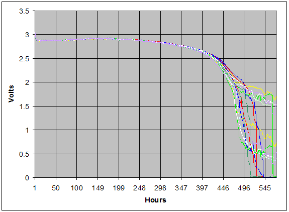
Batteries discharging at a 0.5 mA rate.
Some of the vendors claim their MCUs can run for 20-30 years from a single CR2032. That’s may be true in theory, but not in practice. The first question one must ask is: are the batteries rated for those kinds of lifetimes?
I contacted a number of battery vendors. None guarantee shelf lives over ten years. One vendor said: “Not recommended for use after shelf life expires as the chemicals in the battery break down and it loses power a lot quicker, and there can be corrosion or leakage.”
It’s poor engineering practice to use a component beyond its rated specifications. For this discussion I’ll assume that the maximum achievable lifetime of a system powered by a CR2032 is 10 years, because that’s the life guaranteed by the battery vendors.
Though the war is all about battery lifetime of a mostly-sleeping system, that’s irrelevant for design engineers. The right question – which no one seems to be asking – is: how much useful work can the system do while awake?
“Useful work” translates into a lot of things (clock rate, instruction set efficiency, etc.), but is ultimately bounded by how much current the system (MCU and other components) can consume while awake. It’s is the budget a design engineer has to work with, and cannot be exceeded (on average).
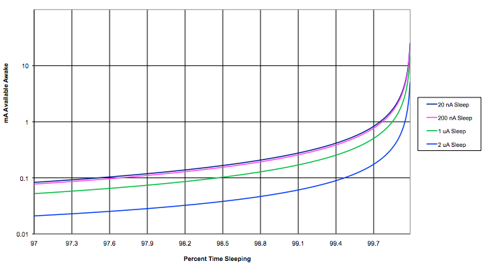
Doing the math, I came up with the following curve, which assumes a ten year battery life for a cell with 225 mAh capacity. It shows the number of mA available while awake, as a function of time spent sleeping and amount of current consumed while sleeping. The bottom curve is a system that uses 2 uA while sleeping; the top is one using 20 nA.
mA available as a function of sleep time and sleep current.
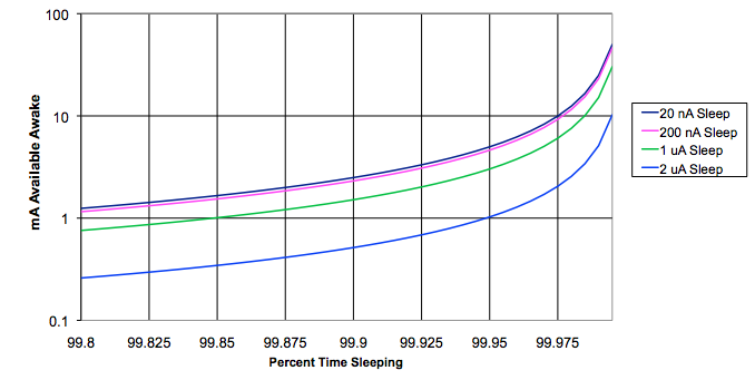
For systems that sleep the vast majority of the time, the following chart blows up the data at the right side of the graph above:
Here’s the key takeaway: Sleep currents are almost irrelevant. Take two MCUs, one that needs 20 nA while sleeping and another that consumes 200 nA. The available awake current is just about the same in both cases. Even one that sucks a microamp while sleeping gives results not much different from an MCU needing an order of magnitude less.
If the system (MCU plus everything else) draws a microamp or less when sleeping we find:
- If your system sleeps 99% of the time you only have a 0.24 mA budget while awake. This means the system is awake 36 seconds per hour over ten years before the battery is depleted. And while it’s awake, you cannot, on average, draw more than 0.24 mA.
- If the system sleeps 99.7% of the time you have 0.8 mA available and are awake 11 seconds per hour. And while it’s awake, you cannot, on average, draw more than 0.8 mA.
- At a 99.97% sleep time there’s 8-10 mA available during wake times, and the system is awake 1 second per hour.
And while it’s awake, you cannot, on average, draw more than 8-10 mA.
It’s useful to think about a total system current budget. For a CR2032 with 220 mAh of capacity running for ten years the calculation is simple:
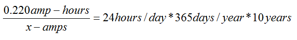
x-amps is the average current consumed by the system over a decade, and works out to 2.5 uA. Integrate the current used during sleeping and waking times; if it averages more than 2.5 uA the battery won’t last ten years. Another way of looking at this, as we’ll see later, is that, since the system sleeps most of the time, the parasitic drains (sleep current plus other circuit drains) cannot exceed 2.5 uA.
2 – On Typical Specifications
Check out the electrical specs of an ultra-low power MCU. Clearly we’re really concerned with the current used in various modes. Surprise! Many only give “typical” (i.e., no worst-case) specifications.
It wasn’t always this way. Here’s an example from TI’s 1976 TTL Databook for the 7447A BCD to seven segment decoder/driver:
. 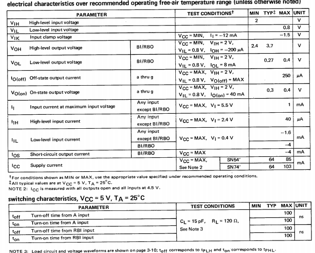
Note that all of the specs have a max or min number, and the data shows what conditions those numbers apply to (e.g., Vol is with Vcc-MIN, Vih=2, Vil=0.8, Ioh=-200 uA).
Admittedly, in the olden days just a few pages were enough to fully document a part. Today a thousand page datasheet isn’t uncommon. Properly characterizing a component isn’t easy.
Here’s another datasheet — it’s from a box of Entenmann’s donuts:

These are worst-case specs. They are guarantees. Contractual terms between Entenmann’s and the buyer. You know what you’re getting.
Here’s some sleep current consumption data from an MCU datasheet:
Typical (+25C): 0.01 uA
Typical (+60C): 0.04 uA
Maximum (+85C): 2 uA
Maximum (+125C): 10 uA
What does that mean? The range covers three orders of magnitude.
Decades ago one of my mentors taught me to never use a “typical” spec; always design for worst case. That has been good advice which I’ve only violated in circumstances where some other data was available or a wide distribution of values was acceptable.
TI agrees. Their datasheet for the LPV521 op amp states: “Typical values represent the most likely parametric norm at the time of characterization. Actual typical values may vary over time and will also depend on the application and configuration. The typical values are not tested and are not guaranteed on shipped production material.” (Emphasis added).
So how does one interpret the current consumption data listed earlier? My first reaction is to use the max (+85C) number as that is, presumably, guaranteed. But that’s 200X the room-temperature “typical” value.
While there’s really not enough data to use for curve fits, an exponential trend line fits pretty darn well, which is hardly surprising given that much of the current is consumed by reverse-biased P-N junctions (think of the Shockley diode equation). But that’s mixing typ and max values, a proverbial conflation of apples and oranges.
I have always assumed “typical” represents an average, or the most-likely value in some probability distribution function. But does it?
I contacted tech support of several semiconductor vendors and asked what “typical” means. The responses were hardly enlightening.
Energy Micro (now owned by Silicon Labs) was the first to reply. They said: “A typical for Energy Micro’s specs is the mean value of the devices measured. So [it’s] not really dependent on the standard deviation. Most CMOS characteristics have a normal distribution, so mean and median are pretty much the same thing.”
That mirrors my expectation, but since bigger standard deviations implies a wider range of values the mean doesn’t tell us much about what to expect. Yet the datasheets for Energy Micro’s ultra-low power MCUs offer (as of this writing) only “typical” current consumption values.
TI weighed in soon after. “‘Typical’ values in datasheets are not taken from probability functions. These are taken from multi-lot characterization testing with the mode being considered the ‘typical’ for a give[n] set of characterization parameters (temperature, Vcc, etc).”
That’s interesting but not terribly helpful. The mode alone tells us nothing about what kind of values one can expect. And TI, like most vendors, only lists the typ value (no min or max) for some parameters on at least some of their MCUs so we don’t get even a sense of the distribution that can be expected.
Microchip responded: “Typical’ is the average of our characterization data.” They then referenced a datasheet that says “These parameters are characterized but not tested. Data in ‘Typ’ column is at 3.0V, 25C unless otherwise stated. These parameters are for design guidance only and are not tested.”
Freescale replied with a link to a Kinetis data sheet. Section 3.8 reads:
A typical value is a specified value for a technical characteristic that:
* Lies within the range of values specified by the operating behavior
* Given the typical manufacturing process, is representative of that characteristic during operation when you meet the typical-value conditions or other specified conditions
Given that typical is “representative of that characteristic” one might assume this means one can expect the part to behave much like the specified typ data. But the example shown on that datasheet just a few lines later rates a current with a min of 10, typ of 70, and max of 130 uA. The standard deviation is enormous. The typ value teaches nothing about the range of values to expect (though, in that example, the min and max tell us everything we need to know; wise engineers will create a design that works properly over that entire range).
|
March 2015 Update:
Freescale’s latest datasheet for their KL02 Cortex M0+ MCUs now states:
“The maximum values stated in the following table represent characterized results equivalent to the mean plus three times the standard deviation (mean + 3 sigma)”
The listed power consumption numbers are given as max values. That’s useful engineering data! Kudos to Freescale. |
NXP told me: “We have not seen a universal definition of ‘typical’, though it has been one of the most commonly used terms in the industry and product. One interpretation would be that ‘typical’ represents ‘material that comes from our production process under standard SPC (statistical process control.)'”
Again, this is interesting and useless, at least for practicing design engineers.
In 2013 an FAE from a large semiconductor vendor told me some of their typical numbers are really marketing tools. Does that mean they can change with the competitive landscape? “Our competitor just dropped their typ specs; we better do the same!”
The bottom line is that the meaning of a “typical” spec is devoid of engineering value. If a spec isn’t guaranteed, it’s not a spec, it’s an aspiration.
Min/max specs are guarantees. “Typical” is not. It’s time for us to rise up and demand better data! Power to the processors! (Well, I guess we want to minimize power to the processors in these applications).
3 – CR2032 Behavior
Some vendors take their MCU’s sleep currents and divide those into a CR2032’s capacity to get huge and improbable lifetimes. But how do coin cells really behave in these low-power applications? No one knows! Even the battery vendors provide only the slimmest amounts of data for systems that go from a deep sleep to needing power for a handful of ms.
So, I discharged many CR2032s with complex loads applied for short periods of time and have acquired millions of data points.
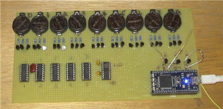
Nine-cell battery profiler using an ARM controller board. Transistors switch different loads on each battery to run various current and time profiles. Loads are low tempco, 1% resistors. An A/D reads battery voltages and Vce of the transistors. A precision reference and software calibrates the entire analog path.
The following results are for 42 batteries from Duracell, Energizer and Panasonic (including other experiments detailed later, I discharged roughly 100 coin cells). For each vendor I ran two groups of cells, each group purchased months apart from distributors located in distant States, in hopes that these represent different batches. (The devices are not marked with any sort of serial or batch numbers).
First, the weird part. Our local grocery store sells these cells for up to $5 each. Yet Digi-Key only wants $0.28 for a Panasonic and $0.40 for an Energizer — in singles. Duracells are harder to find from commercial distributors, but I paid about a buck each from on-line sources (e.g., Amazon).
I found little battery-to-battery variability (other than one obviously bad Panasonic and one bad Duracell), little vendor-to-vendor difference, and likewise different batches gave about the same results.
What parameters matter? Chiefly, capacity (how many milliamp-hours one can really get from a cell), and internal resistance, which varies with capacity used.
All of the vendors say “dead” is at 2.0 volts.
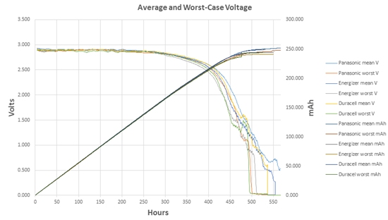
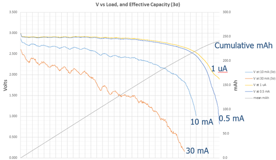
The following graph shows the average voltage for the batteries from each vendor, as well as the worst-case voltage from each vendor, as they discharge at a 0.5 mA rate. The curve ascending from left to right is the cumulative capacity used. By the time 2.0 volts is reached the capacity variation is in the noise. I found it averaged 233 mAh with a standard deviation between all results of 5 mAh. Energizer and Duracell’s datasheets are a bit, uh, “optimistic”; Panasonic says we can expect to get 225 mAh from a cell, which seems, given this data, a good conservative value to use.
But in practice you won’t get anything near that 225 mAh.
It’s useful to model a battery as a perfect voltage source with an internal series resistance, as follows:
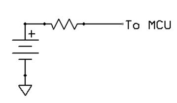
As cells discharge their internal resistance (IR) goes up. Actually, this is not quite correct, despite the claims of all of the published literature I have found. Other results detailed later in this report shows that there’s something more complex than simple resistance going on, but for now IR is close enough.
The next chart shows average IR for each vendor’s products, plus the IR’s standard deviation.
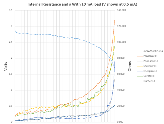
Internal resistance and its standard deviation.
So what does this all mean to a cautious engineer? The IR grows so quickly that much of the battery’s capacity can’t be used!
First, the average IR is not useful. Conservative design means using worst case figures, which we can estimate using the measured standard deviation. By using three sigma our odds of being right are 99.7%.
The following graph combines the IR plus three sigma IR. Depending on the load, the drop across the battery’s internal resistor will reduce the voltage delivered to the system, as shown:
Voltage delivered from battery depending on load.
If a system, when awake, draws just 10 mA 88% of the battery’s capacity is available before the voltage delivered to the load drops to 2.0. It’s pretty hard to build a useful system that only needs 10 mA. Some ultra-low power processors are rated at 200 uA/MHz with a 48 MHz max clock frequency — almost 10 mA just for the CPU.
With higher loads, like any sort of communications, things get much worse. Bluetooth could take 80 mA, and even Bluetooth LE can suck nearly 30 mA. At 30 mA only 39% of the battery’s rated capacity can be used. An optimist might use two sigma and suffer from 5% of his system’s not working to spec, but that only increases the useful capacity to 44%. The battery will not be able to power the system long before it is really “dead,” and long before the system’s design lifetime.
And long before the time MCU vendors cite in their white papers.
(Some MCUs will run to 1.8 volts, so vendors might say my cutoff at 2.0 is unfair. Since battery vendors say that 2.0 is “dead” I disagree. And, even if one were to run to 1.8V there’s less than a 5% gain in useful capacity.)
4 – Leaks and Drains
The microcontroller doesn’t live in a vacuum; it’s part of the system. Other components draw power, and it’s the design engineer’s job to evaluate those drains. Some may be surprising.
I have a lot of evaluation boards here; many are designed to show off the long-battery-life aspects of a particular processor. It’s interesting to examine the designs. I put one of the boards under a microscope and looked at some of the ancillary parts. There’s a 22 uF decoupling capacitor. No real surprise there. It appears to be one of those nice Kemet polymer tantalums designed for high-density SMT applications.
The datasheet pegs the cap’s internal leakage at 22 uA. That means the capacitor draws a thousand times more power than the “typical” value cited for the dozing CPU. In fact, the cap alone will drain the battery in under a year!
Engineers may argue that 22 uF is a really high value. But that’s what the silicon vendors suggest. Silicon Labs application note AN0002 Rev 1.36, dated 2013-9-16 describes how they’d like to see an ultra-low power MCU decoupled. Over 20 uF is required.
A capacitor has parasitics, and in simplified form looks like this:
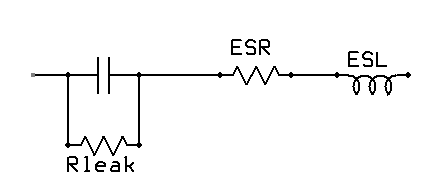
Usually the ESR (equivalent series resistance) is pretty low; for caps that are not wound ESL, too, is low. One would hope that Rleak would be infinity. Alas, that’s far from true. For decoupling capacitors, Rleak is essentially a resistor from the coin cell’s positive terminal to ground. For all of the years the MCU is sleeping, Rleak is discharging the battery.
Section 5 of this report gives more information about selecting decoupling capacitors; a poor selection is guaranteed to drain the battery in a short period of time. Tantalums leak far too much to use as decoupling capacitors. Most MLCCs won’t work, either. Use the advice in that section to specify the right decoupling parts.
There is good news for designers: if the batteries start failing at the five or seven year mark, probably no one will remember who is at fault.
What about other sources of leaks? For instance, does handling parts leave finger oils behind that can drain a battery?
A lot of on-line pundits bloviate that the leakage problem is a big factor; experience shows that the more an Internet poster asserts that X is an indisputable fact, the more likely it’s not. (A century and a half ago, Charles Darwin noted that “ignorance more frequently begets confidence than does knowledge.”) This is engineering, not speculation, so I decided to run some experiments to see how significant these leaks are in a digital circuit. But how to do so? Clearly, to get meaningful data one must measure these drains to a resolution much better than the 20 nA (nanoamps) or less some of the MCUs use while sleeping.
One could use a DMM to measure leakage in ohms. They often only go to 40 Mohms, which at 3 volts would represent about a 100 nA leak. That’s too crude. The uCurrent tool can resolve to a single nA, which is probably adequate, but at 1 nA it generates only a single mV, which is pushing the resolution of most DMMs pretty hard.
So I built a sample and hold circuit (S&H). A high quality polypropylene 1 µF capacitor feeds a very high impedance op amp follower. Put a component whose properties you want to measure around the cap, charge it up, and watch the discharge curves by reading the op amp.
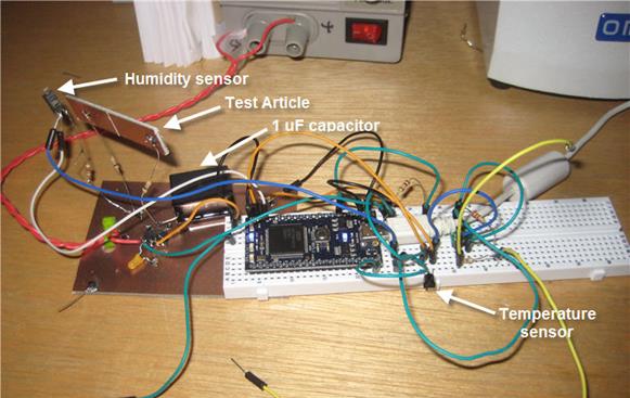
Sample & Hold circuit to test for very low leakages
I used an LM662 op amp, which has a 2 femtoamp (typical – no max is listed) input bias current. One fA is a miniscule 10-15 amps, a millionth of a billionth of an amp, or about 6000 electrons/second, so its effect on the capacitor is minimal. The amplifier’s inputs and the cap’s connection are all made in the air. A Cortex M3 controller with a 12 bit A/D reads the amplifier periodically, as well as temperature and humidity sensors, and shoots the results to a PC via USB for logging.
Measuring the time constant with a 10 Mohm resistor across the capacitor proved the circuit worked as expected. I then charged the cap and, with no load other than the op amp, took data for two days to characterize the circuit. The results are summarized in the following graph.
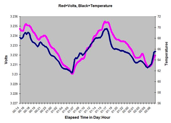
The 12 bit A/D is at the extreme end of its resolution so each data point is the average of 5000 samples.
Clearly the voltage is highly dependent on temperature. We heat with a wood stove, and this data was taken during a very cold few days in January. The dips bottomed out in the morning as the house cooled all night; they veered up when I restarted the fire.
My goal was to measure the resolution of the circuit, but the results are very hard to interpret as it’s tough to separate out the temperature effect. Has it discharged at all?
Plotting voltage against temperature:
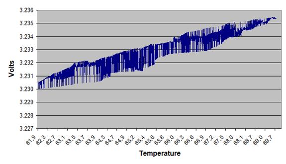
The voltage across a capacitor that is discharging over time is:
Where V0 is the initial voltage on the cap and t is the elapsed time. Taking the natural log and rearranging we get:
. 
R is the effective resistance that bleeds charge from the capacitor. Some of that “resistance” is due to the bias current going into the op amp; some is in the cap body itself, and some is from leakage into air.
Ohm’s Law converts R to amps. If the voltage decayed by 1 mV this gives 6.6 fA of leakage from all sources. Alternatively, by plugging 10 fA into the equation the voltage would have decayed to 3.228, which would have been very easy to see. So the S&H can resolve better than 10 fA. That’s many orders of magnitude lower than any leakage that would concern us in designing a low-power system.
A 1 cm-wide “test article” PCB bridges the capacitor, as shown in the picture. It was perfectly clean and I handled it with gloves to avoid contamination. There’s a 0.5mm grove whittled across the board. How much does FR-4 material leak in 30% relative humidity? I have no idea. But the S&H confirmed that it’s less than 10 fA.
Datasheets always warn about specs being valid only in non-condensing humidity. How important is that? I boiled some water and collected the condensate to emulate the sort of moisture that likely makes up water vapor in the air, and bridged the test article’s insulating gap with a 2 mm diameter drop. Just over 1 µA flowed, similar to figures available on-line. Conductivity is measured in units of ohm-meters, so there could be a lot of µA flowing in a real PCB with more surface area under water.
Despite extensive searches I couldn’t find any useful data about how the conductivity of a PCB is affected by humidity. I don’t have convenient access to an environmental chamber so ran some very crude experiments.
I covered the test article and humidity sensor with a plastic coffee can with a hose protruding from the bottom. Taking data in real time (with humidity and voltage readings displayed on the PC) I huffed and puffed into the hose. At 70% relative humidity the test article’s leakage went from under 10 fA to 13 pA, a jump of three orders of magnitude. At 80% (the highest I was able to achieve) that went to 20 pA. Now, this is over a 1 cm long gap, so a better metric is 20 pA/cm. A board with 50 cm of track would experience about 1 uA of leakage, enough to eat almost half of a CR2032 battery’s 10 year power budget of 2.5 uA.
There are two mechanisms for leakage due to humidity. The first is through the moist air that separates two tracks or terminals. The second is via adsorption of water molecules on the surface of the PCB. Other contaminates like dirt that might have a very low conductivity can adsorb water molecules and reduce the board’s resistance. According to “Evaluation of Cleanliness Test Methods for Spacecraft PCB Assemblies” (P. E. Tegehall and B. D. Dunn, ESA STM-275, October 2006) a water film just 20 molecules thick will have a conductivity that is only an order of magnitude lower than that of bulk water.
What about contamination? Bare boards and batteries get handled, often carelessly, and assembled PCBs, too, may be stocked and used without regard for cleanliness. A common concern is leakage due to finger oils. Lots of on-line pedants complain that this is a very significant problem. But hard data is scarce.
I grabbed a bottle of my wife’s Jergens Dry Skin Moisturizer, Original Scent, and spread the thinnest layer I could on the test article insuring the entire 1 cm long gap between copper foils was bridged. The leakage was too much to measure with the S&H. But 24 hours later, after the volatiles evaporated, it was down to 180 pA. After another day the leakage hadn’t changed. That’s 0.18 nA, not much, but is over a short 1 cm length, and could add up with lots of contaminated PCB tracks.
After cleaning the board with isopropyl alcohol the leakage was 2 pA, the better part of three orders of magnitude worse than when I tested the fresh, uncontaminated board. More cleaning didn’t help. The Moisturizer had effected some change to the PCB. Happily, 2 pA is a very small value, though it could be disastrous to some analog circuits.
Next came the finger oil test using both lovely soft female fingers which an hour earlier had been gooped up with the Jergens, as well as nasty crackled Jergens-free male fingers. We touched the test article gently, rubbed some, then smeared furiously. In no case did the leakage exceed 8 pA. Now, that’s enough to cause the S&H’s output to droop by more than 50 mV in 20 seconds, devastating in a sensitive analog sample and hold circuit. But it’s not enough to have any measurable effect on battery life.
Since containments can increase the adsorption of water molecules I exposed the finger-oily test article to 80% relative humidity. The numbers rocketed to 65 pA, three times the humidity result with a clean board. Again, 65 pA is nothing, but multiply your track lengths by the 1 cm long test article used in this experiment.
Could leakage come from salts left behind from perspiration? I mixed up a solution of warm water and salt, supersaturating the solution to the point where the water could hold no more salt, and completely coated the 1 cm gap in the test article. Wet, the leakage was unsurprisingly too huge to measure with this circuit. But after the water dried, it dropped to under 50 fA at 30% ambient relative humidity.
That’s with dry salt. Subjecting the test article to 50% relative humidity caused the leakage to jump to 2 µA.
This is a very contrived test. It’s hard to believe that handling a board would leave so much salt behind (as confirmed by my finger-oil experiments).
Using a fresh test article, I tested several kinds of rosin, first soldering while taking care to insure the rosin smeared across the gap in the copper foil, and later just gooping bulk rosin across it. The worst leakage was 2 pA. Adding 80% humidity simply boosted the number to 20 pA, the same result for a clean test article.
Interestingly, careful cleaning with isopropyl alcohol boosted the drain to 32 pA over the 1 cm gap length. Recleaning even more carefully got that down to 4 pA. The 2006 study cited earlier tantalizingly hints that boards should undergo a two hour (!) bath in an ultrasonic cleaner.
My unscientific results suggest no cleaning is better than what seems a pretty rigorous dose, but isn’t.
What about solder mask? I reran the salt water experiment on a PCB whose traces were covered by a solder mask. Even sopping wet, the leakage was under 10 fA. The finger oil experiments, too, gave leakages too low to measure. Ditto for smearing Jergens on the board. The solder mask seems to be a nearly-perfect insulator, though of course there will be no mask around solder joints.
Here are the results:
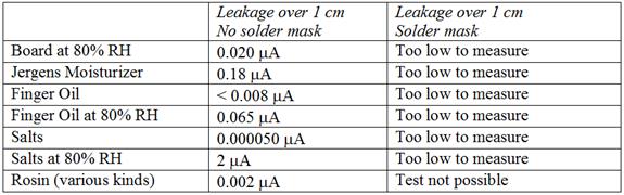
To summarize, assuming no sensitive analog circuits, the experiments showed:
- Finger oils are not a big deal.
- Humidity matters if there’s a lot of exposed track and the humidity is very high for a long time.
- Condensing water is bad.
- Cleaning is hard, and may cause even worse problems.
- Solder mask solves essentially all of the leakage problems.
The takeaway is that the usual practice of putting a layer of solder mask on a PCB eliminates leakage problems related to battery-powered MCUs. Don’t worry about assemblers mishandling the board or the battery. There will be leakage around exposed pads, but outside of extreme environments that should have no noticeable effect on battery life.
5 – Decoupling, and Using a Capacitor to Boost Vdd
Capacitors leak. Some a lot. What type of decoupling capacitor should we use? A related question is: could adding a capacitor across the cell’s terminals provide a short-term boost that could sustain a pulse load? It’s not hard to show mathematically that the answer is “yes.”
But the math is irrelevant. In engineering we’re always faced by conflicting needs and what appears a simple solution sometimes isn’t.
As shown earlier, it’s useful to think of the battery as a zero impedance source with an internal resistor between it and the terminal. That resistor’s value increases as the battery capacity is drained. If it were 50 ohms and the system needed 10 mA the terminal voltage is down by half a volt, often enough to cause the MCU to crash. Add a big capacitor, as in the following diagram, and a short pulse load can draw on the charge stored in the cap.
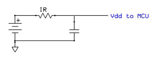
In a TI white paper (“Coin Cells and Peak Current Draw“) the authors conclude that this is a viable solution. They show a case where a capacitor must sustain a 30 mA load for 1 ms. An 87 uF capacitor will do the trick, though they recommend 100 uF since no one makes 87 uF devices.
There are a couple of problems with this conclusion.
First, the capacitor leaks. It’s always across the battery terminals, so is sucking juice, depleting the battery, even during long sleep intervals. How much leakage? It depends on a number of factors, including dielectric material. Let’s consider tantalums, which offer great capacitance versus cost figures. The following table shows the numbers for a 100 uF part. (For tantalums it’s usual to rate leakage in CV, where V is the rated, not the applied, value.)
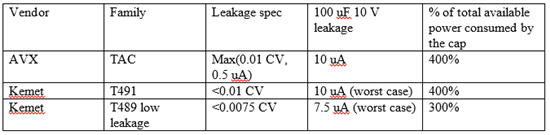
The last column is the most telling. Given that the average current draw over 10 years cannot exceed 2.5 uA, just the capacitor’s leakage will suck the battery dry in a fraction of a decade.
Who would have thought that a cap could leak more than Edward Snowden?
How about a better part? The best low-leakage capacitors with the C values needed are MLCC. MLCC leaks are specified in ohm-farads:
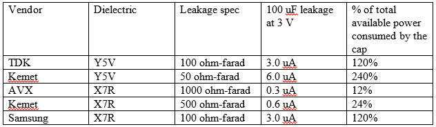
It’s clear Y5V dielectrics can’t be used. Select a more expensive X7R device. And, one must be careful which X7R is selected as some leak as badly as Y5Vs.
Takeaway: be really careful which decoupling capacitors you choose!
The X7Rs exhibit better temperature stability, which has always been the primary reason to use them, but not as a function of leakage! Here’s a typical graph of normalized leakage versus temperature:
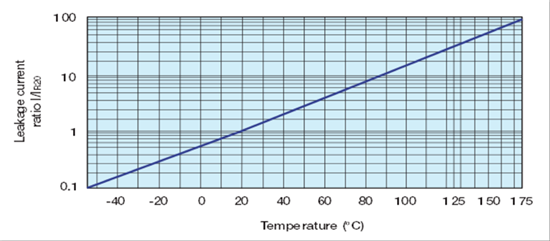
A system that has to run over wide temperature extremes may leak two orders of magnitude more than shown in the previous table; that sweet AVX spec’d at 0.3 uA suddenly looks like a moderately low-value resistor. But even over room temperature, say 20 to 30 degrees, plan on twice the parasitic drain than specified. In the case of the AVX a quarter of the battery is lost to the capacitor.
It gets worse.
MLCC devices derate themselves. As the applied voltage increases, the effective capacitance decreases. Murata has a tool that helps model this, and here’s the result for 22 uF parts:
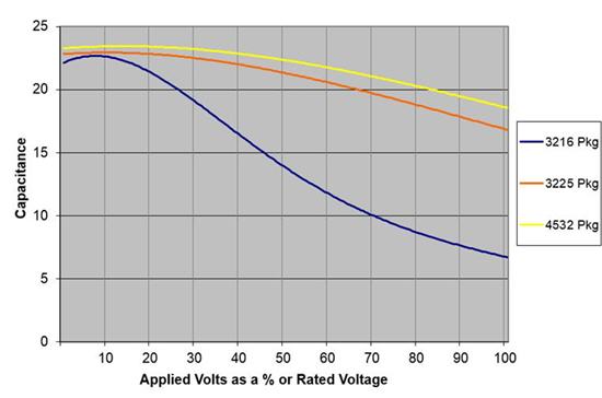
If space is precious you have few options. Apply 3 volts to a nice small 6 V 3216 device and only half the capacitance is available. The TI paper specifies a 100 uF part, but in this package you’d have to use 200 uF. Alternatively, one could use a higher-voltage (bigger and more expensive) device, or use a larger package as shown in the graph.
Capacitors have tolerances, and though X7Rs are generally +/- 20%, one still has to figure that in:
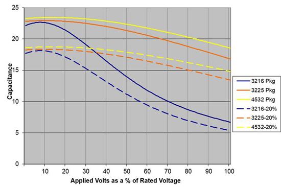
Figure on an even bigger capacitor to deal with tolerance.
Perusing various sites it’s rather astonishing how few capacitor vendors specify leakage. A lot of them claim “low leakage” but don’t give numbers. That’s about as useless as a campaign pledge.
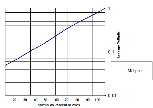
Kemet’s excellent “Application Notes for Tantalum Capacitors” does show how derating the voltage can help. Operate at the cap at a third of the rated voltage and the leakage will typically decrease by an order of magnitude. Go to ten percent of the part’s rated level and leakage dives by another factor of five. But in a three volt system that means a 30 volt capacitor — bigger and pricier.
These deratings are “typical” numbers. Use with caution.
So, despite the problems with capacitor deratings and leakages, can use use one to temporarily sustain a Vdd high enough to keep an MCU from crashing during a brief waking period?
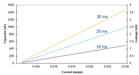
The following graph shows the required capacitor, at 20 degrees C, for 10, 20 and 30 ms pulses with various loads, ignoring all of the complicated effects noted above. You’ll have to factor all of those parameters in as well, which, as we’ve seen, can more than double the required uF. The leakage numbers are based on that nice AVX component. Though the TI paper uses a capacitor to boost power for 1 ms, for Bluetooth and other protocols tens of ms are more likely.
So we’ve done the math, and have figured out what size capacitor to buy. Let’s ignore all of the unpleasantness and assume that a 100 uF part fits the bill, and that we’re using a low-leakage AVX part. They’re $14.50 each! Neither Digi-Key nor Mouser has them in stock, and quote a 25 week lead time as of this writing. Digi-Key does have a 50 V version available today, but that will set you back $36.54.
A complete Raspberry Pi with 700 MHz ARM processor and half a gig of RAM costs less than that capacitor.
Maybe this is a government project where costs don’t matter. Using the graph above we pick off a 400 uF part for a 10 mA 20 ms load (remember, this is before all of the derating that must be done). The leakage will eat about half the battery capacity. And, the capacitor doesn’t exist; the biggest such part on the market is 220 uF. You can’t buy a bunch of smaller parts and parallel them, since the leakage will go up.
What about a supercapacitor? These are astonishing devices that offer farad-levels of capacity. Alas, the lowest-leakage supercap I can find is from Cap-xx, and they quote 2 uA at 23C, doubling at 70C. That’s impractical since even at room temperature it’ll eat just about the entire 2.5 uA current budget.
Summing up, in the use case I’ve described (ten years of system life from a coin cell) it’s impractical to get a short Vdd boost from a capacitor across the battery.
6 – Running Fast to Save Power
There’s an equation that’s constantly bandied about when talking about power consumption of electronic devices. If you’re designing battery-operated ultra-low-power devices, it’s critical that you, well, ignore it.

Engineers’ eyes light up by the V-squared term; they immediately start looking for a way to lower Vdd to get more battery life.
As we’ll see there might be some benefit to dropping the power supply voltage. But this equation is irrelevant to ultra-low power systems because it measures power — watts — not current. High-performance systems live and die by power; have you seen the cooling towers on desktop CPUs? Battery operated systems are constrained by battery capacity, which is measured in amp-hours; typically the units are milliamp-hours (mAh). Power is not the issue for figuring battery lifetime.
Think in terms of current.
The following graph shows how one of Microchip’s nice low-power MCUs uses current as a function of clock frequency:
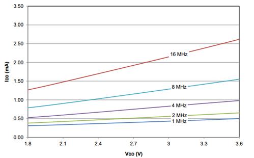
Note that doubling the clock rate from one to two MHz uses much less than a twice the current. The reason is that the CPU is only one of the powered components. Memory and peripherals suck coulombs, too, and not all of these needs vary with clock frequency. There’s a static, constant draw, and one which is a function of frequency. It’s not hard to pick points off the graph at 3.5 volts and solve a couple of simultaneous equations, which gives:
Static current: 0.39 mA
Dynamic current: 0.11 mA/MHz
At one or two MHz most of the current is used by static loads. At higher frequencies the constant draw is still significant. It’s clear that wise designers will run at the max possible clock rate to get back to sleep as quickly as possible. This is the advice given by all of the MCU vendors.
And it’s wrong. Or at least naïve.
Remember how a battery’s internal resistance increases as it is depleted? Here’s the graph again, which shows the voltage delivered by the battery depending on load:
If one were to follow the advice to run as fast as possible, coming out of a sleep state means the system will be drawing perhaps a lot of current. Over time, the battery’s internal resistance will increase to a point where it may have a lot of capacity left, but cannot power a speedy current-hungry MCU. Wake up, and Vdd drops below the minimum allowed, so the processor crashes.
At least one series of MCUs advertised for ultra-low power operation consumes 200 uA/MHz, maxing at 48 MHz. That’s about 10 mA just for the MCU. The battery might not be able to sustain a 10 mA load, but at 1 MHz — 200 uA – it can have plenty of life left.
The moral is to wake up at a low clock frequency. Ramp it up while watching Vdd, stopping a bit above the MCU’s cutoff point. Be sure to factor in the needs of I/O you’ll be powering up.
Alternatively one could apply some a priori knowledge (e.g., track consumed mAh and use data such as in the graph above to estimate the operating point) to set the clock frequency.
But if you take the vendors’ advice and wake up at full throttle, the useful battery lifetime may fall far short of your design goal.
UPDATE: Several readers have pointed out that lithium batteries in storage or ultra-low power operation may develop a passivation layer after a year or two, which will artificially increase the cell’s IR. The way to get rid of the passivation layer is to drop a high load on the cell till the battery’s voltage recovers. Some info on-line suggests that only certain kinds of lithium cells suffer from this but information is sparse. This link describes the situation.
So the advice above is good: wake up in a low-power mode as described, but if it’s early in the cell’s life and a high IR (low voltage) is found, drop a heavy load on the cell till it recovers. This could be done by powering up a transmitter or doing a flash write. Be cautioned, though: don’t apply a load so high that the MCU crashes.
7 – Dropping Vdd to Cut Current and Increase Battery Life
When trying to maximize the amount of energy one can get from a battery powering an MCU it’s important to remember that we’re interested in current, not power, since battery capacity is measured in mAh. The equation for power has a hugely-seductive V squared term, but when we’re (correctly) thinking about current, voltage’s effects are linear.
So, does it make sense to exploit current’s linear relationship with voltage?
Consider the following graph for one of TI’s nifty MSP430 MCUs:
The curves above show a substantial reduction in current as the Vdd decreases. Even at 1 MHz, where the graph isn’t very dramatic-looking, there’s about a 2X improvement by scaling back the MCU’s supply voltage. So this sure looks like a great place to cut coulombs.
It’s tempting to put in a low-dropout regulator to reduce Vdd to 2.0, but I can’t find any linear devices whose idle current during the MCU’s long sleep states won’t deplete the battery. Smarter parts can work, like TI’s $0.80 TPS 62736 buck/boost converter that needs only 400 nA for Iq. It does require an inductor, but those are only about 7 cents in quantity. Touchstone’s TS3310 (now owned by Silicon Labs) has even better specs.
But long-lived systems are almost always asleep. A device that has to run for a decade off a coin cell will be snoozing well over 99% of the time. The graph above is active current; cut that by half, and factor in the 1% or less awake time, and it’s clear that there’s really no real benefit to scaling Vdd.
What about cutting Vdd during the 99% of the time when the processor is sleeping?
Most MCUs offer a number of sleep modes that each have differing energy needs. Some show a very small difference in worst-case consumptions; it’s common to find in a deep sleep only a 20% variation between 3 and 2 volts. 20% may be enough to justify an extra dollar’s worth of buck/boost parts as that could add a couple of years to the operating life of a very-low-power system. But remember that a ten-year life means the system’s average draw from a CR2032 can’t exceed 2.5 uA. The TPS 62736 will eat 400 nA of that budget.
One vendor shows curves for “typical” sleep needs, and there’s about a 2X difference between 3 and 2 volts, which sounds promising. But under 3V the curve is labeled “limited accuracy.” Combine the meaninglessness of “typical” numbers with “limited accuracy” and I, for one, have no idea how to interpret the data. One wonders if the datasheet was created by marketing folks rather than engineers. “Take it from us, in some modes, it’s possible, based on a statistically meaningless set of observations, that the part might, if coupled to the wings of angels, work in your application.”
Unfortunately, most datasheets don’t spec out the difference in sleep current as a function of voltage, so it’s impossible to know what benefits, if any, accrue from voltage scaling.
As always, read the datasheets carefully and do a full analysis of your design goals.
8 – Most Brown-Out Reset Circuits Don’t Work
Low-power MCUs usually have a built-in brown-out reset (BOR) circuit. Unfortunately, most are poorly designed and/or lightly documented and should not be used.
One popular ultra-low power MCU, from a vendor who noisily advertises two to three decades of coin cell operation, has a BOR which is off by default. On, it requires somewhere between 8 (typical) and 16 uA (worst case). Remember that, for a decade of life from a CR2032, the system’s average power draw cannot exceed 2.5 uA. Even if one were to foolishly use the typical number, the BOR by itself will deplete the battery in just a couple of years.
Another vendor, pushing extremely-low power ARM parts, rates the BOR at 0.49 to 1.26 uA — typical. There’s no max listed; there’s not the slightest guidance of what statistical distribution one can expect when making thousands of systems. 1.26 uA eats half the 2.5 uA budget.
In another case the datasheet reads about the BOR: “In the deeper sleep modes, this will contribute significantly to the total current consumption.”
As Deming said: “In God we trust, all others bring data.” They didn’t, and it strikes me as risky to rely on divine intervention instead of careful analysis. I’d be wary of using these uncharacterized parts in long-lived applications. As always, read the datasheets pessimistically and carefully.
When does the BOR interrupt occur? In some cases the voltage range is very wide; an example is an MCU where it is listed as 2.05 (min), 2.2 (typ), and 2.35 volts (max). Doing worst-case design you’d have to assume that the BOR may occur at 2.35 volts.
The following graph is one I have used before; it shows the voltage a CR2032 can deliver as it discharges as a function of load.
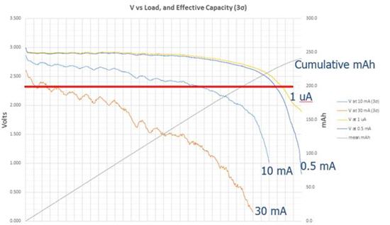
The 10 mA load line is pretty common for an awake MCU with enabled peripherals; 30 mA is not unexpected if there’s any sort of wireless comm going on. The heavy red line is at 2.35 volts, the max value where we may see a BOR interrupt. Note that in this case the BOR circuit will signal a dead battery, if there’s a 30 mA load, shortly after you ship the product. With a 10 mA load the battery-dead indication happens when there’s still 31% capacity left.
In other words, the BOR circuit is useless.
A much better alternative is to leave the BOR off and use the A/D. Wake up from time to time, apply a load similar to what the system normally needs when awake, and read Vcc. If it’s near 2.0, then signal a battery failure (or take whatever action your system needs in this situation).
If such a reading is taken once every ten hours (surely, more often than needed), and 10 mA were pulled for 1 ms during this reading, over a decade this eats only 0.03 mAh, or 0.01% of a CR2032’s capacity. And, by manually reading the A/D a more nuanced approach to battery management is possible than by relying on a single, poorly-controlled, BOR voltage.
9 – Reverse Battery Protection
How should you design the system to protect it from well-meaning users trying to change the battery?
A typical coin cell battery socket looks like this:
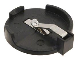
Inexpensive coin cell holder.
It’s cheap, it’s easy, it mounts well on a PCB, and it’s a disaster. A confused user, poor instructions, perhaps a martini-induced brain fart, and an upside down battery will fry all of the sensitive electronics.
I saw a system not long ago that used a small signal diode to insure the electrons flow in the right direction. But that sort of a design is a catastrophe for these systems. It takes 0.7 volts right off the top; as the battery discharges it’s not long before there’s not enough voltage to keep the MCU going, even though the battery is a very long way from being dead.
Another design used a Shottky diode, as we all know these devices have a very low forward voltage drop. Anecdotally people talk about 0.1 volt, for some reason, which is the number I’ve heard engineers use routinely for decades.
But that’s simply not true. Here’s the forward voltage drop for a typical Shottky diode:
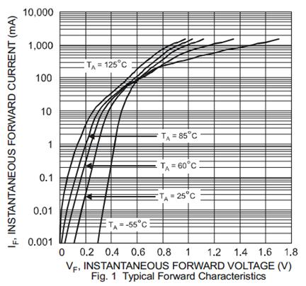
Shottky diode forward voltage
Sure, you can expect 0.1 V or so… at 0.005 mA! At more realistic currents (10 to 30 mA or so) that jumps to 0.4 V at room temperature.
If the protection diode drops 0.4V, then once the battery drops below 2.4V the system gets 2.0V. It can no longer provide enough voltage to keep the MCU alive. Remember the graph that showed typical voltage from a CR2032 for various loads? This is the same plot with a red line at 2.4V.
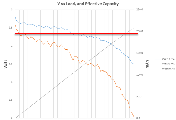
The useful battery capacity with a diode is above the red line.
Once the battery voltage falls below the red line the MCU will be starved for electrons. In the case of a 30 mA load pretty much the entire capacity of the battery is lost. Even with a 10 mA load over half the battery is unusable.
A much better solution is a one that won’t properly engage the battery if the cell is inserted backwards. The following part from Memory Protection Devices
is a good example:
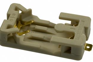
A better coin cell socket.
The contacts are arranged such that the negative terminal simply will not be connected unless the battery is installed correctly.
It’s $0.25 more than the socket shown before. But if you care about the customer experience, use a socket that will simply leave the system unpowered when the battery is inserted backwards.
10 – UL Coin Cell Requirements
Bob Snyder sent me the UL rules for using coin cells in products.
There are a number of requirements that must be met to obtain UL approval in devices with user-replaceable batteries. For instance, the device must be marked “Replace Battery With (Battery Manufacturer’s Name or End-Product Manufacturer’s Name), Part No. ( ) Only. Use of another battery may present a risk of fire or explosion. See owner’s manual for safety instructions.”
I have never seen this on any product that uses coin cells.
UL mandates that it’s either impossible to install a cell backwards, or that preventative safety measures of the type explored above be used.
In many applications coin cells are used just to maintain RAM’s contents when the mains power is down. UL is very concerned that the battery cannot be reverse-biased when the power supply is feeding memory, so requires that either two series diodes, or a diode with a current-limiting resistor, be placed between the battery and the rest of the circuit, as follows:
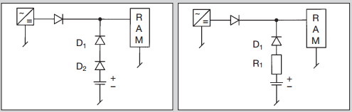
Why two diodes? UL’s ultraconservative approach assumes one may fail. The resistor is to limit current if the diode in that circuit shorts.
In most cases the first circuit won’t work; even two Shottky diodes will drop about 0.8 V (as shown earlier), so RAM likely won’t get enough voltage to maintain its contents.
The second circuit requires a resistor that limits reverse current to a UL spec of 25 mA for most coin cells. But how is one to compute the proper resistance? You need to know the battery’s internal resistance (IR) when reverse-biased, and I cannot find any documentation about that. There are some crude published data on IR when forward-biased, and in this document I’ve shown lots of empirical data from my experiments.
One could assume the battery’s IR is zero, which would certainly give a nice worst-case result, but I decided to explore this a bit more.
I applied a power supply to a CR2032 and measured the current flow when the supply’s voltage was 0.5, 0.75, and 1.0 volts above the battery’s unloaded voltage. The battery was contained in an explosion-proof container. Well, actually, an old coffee can, but it sure would have been fun to hear a boom. Alas, nothing exciting happened.
From that it was easy to compute IR, which is displayed in the lower three lines on the following graph:
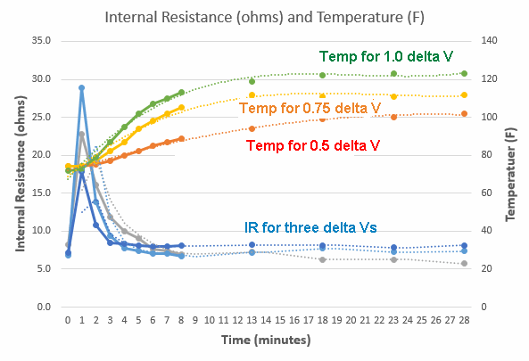
(I took data every minute for the first 8 minutes, and at 5 minute intervals thereafter. The dotted lines are trendlines.)
Strangely, the internal resistance spikes immediately after the power supply is applied, then quickly tapers off. In a matter of minutes it falls to six to eight ohms. The data is very similar for when the power supply was 0.5, 0.75 or 1 volt above the cell’s unloaded voltage; that’s not unexpected if one assumes this really is resistance and not some complexity arising from the chemistry.
The top three curves are the battery’s temperature. Unsurprisingly, temperature goes up with the voltage difference. Given UL’s dire warnings about catastrophic failure I expected more heat, but the max encountered was only about 50 C, far lower than the 100 C allowed by UL rules.
Now, this data is for a single battery, so be wary, but it does conform to the IR characteristics I measured for forward-biased cells.
Probably the only decent solution, if you don’t want to use a socket as described above, is to use a FET to protect the circuit if the battery is installed backwards. TI has a nice application note about this.
This leads to another question: to get more capacity, can we parallel two or more coin cells? UL is silent on the subject. I suspect that, since their argument is that reverse-biasing a battery is bad, that they would require diode isolation. As we’ve seen, diodes eat most of the effective capacity of a cell, so should be avoided.
From a non-UL, purely electronics standpoint, what would happen?
This is a debate that rages constantly in my community of ocean-sailing friends. The systems on our sailboats run off large, often lead-acid, batteries. On my 32 foot ketch, the fridge sucks 50 Ah/day, the autopilot another 50 Ah, and the radar, well, at 4 amps we don’t have the power to leave it on all of the time. All of this comes from two 220 Ah six volt golf-cart cells wired in series. After a day or so of running the systems we have to fire up the engine to recharge, which everyone hates. Can we wire two banks of golf cart cells in parallel? I have heard all sorts of arguments for and against, but many do wire their systems that way and get good results.
What about coin cells?
My experimental data shows that the maximum difference in unloaded voltage for fresh CR2032s is about 0.25 volt. This is true for a single brand and between brands and lots.
With two paralleled cells of unequal initial voltages, the lower-voltage battery’s small IR will discharge the higher-voltage cell rapidly until both batteries are at the same voltage.
LiMnO2 cells have a very flat discharge curve till they approach end of life. Discharge one by a quarter volt and you have lost around 200 mAh of capacity, or about 90% of the cell’s 220 mAh rating. So the battery with the higher voltage will quickly run down to 10% reserves. Most of its capacity is thrown away.
But it gets worse. Once heavily discharged the battery’s voltage is at a knee on the curve and falls rapidly. The one that seemed better, with a higher voltage when first installed, now acts as a load on the other!
They essentially suck each other dry. So don’t put these in parallel.
11 — Battery Droop Over Time
Suppose one applies a fixed load to a coin cell for a short period of time. Does the battery voltage change? That’s a special case of a broader question: everyone uses internal resistance (IR) to characterize these cells. Is IR really an accurate way to model their behavior?
For this experiment I discharged 9 CR2032s. Most of the time there was only a 0.5 mA background load to run the batteries down, but every two hours the test jig applied either a 10 mA or a 30 mA load for one second. That is, at the 2 hour mark the cells saw a 10 mA load; at four hours it was 30 mA. The system read voltages immediately after applying the load, every 10 ms until 100 ms went by, and then at 100 ms intervals.
Here are the results for 30 mA. The horizontal axis is time, but I left it unlabeled as it could be weeks, months or years depending on the discharge profile. The blue line is the battery’s loaded voltage; other lines are the internal resistances during the one second interval:
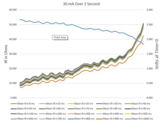
Note that the bottom red line is the mean IR for 9 batteries at 0 ms, immediately after slamming on the load. All of the other data points are pretty tightly grouped. In other words, the IR goes up significantly (about 10%) milliseconds after the load shows up, but there’s little change after that.
In other words, IR is not an accurate model of coin cell behavior. It’s not bad; for an engineering analysis it’s probably close enough. But there is some other effect from the battery chemistry going on.
The results are clearer with less data. Here the red line is the IR at 0 ms; grey is at 10 ms, and yellow at 1 second:
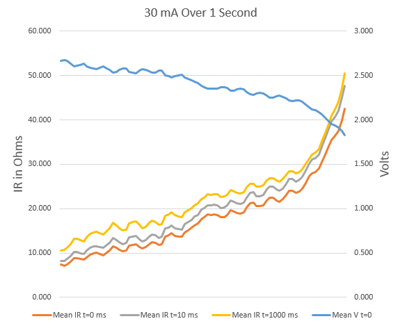
Especially nearing the end of life we can see a big increase in IR from 0 to 10 ms, but not much more from 10 ms to 1000 ms. Yes, the effect is different when the battery hasn’t run down too much, but then the voltage is higher and IR is so low the increasing IR isn’t particularly important.
With a 10 mA load the results are about the same:
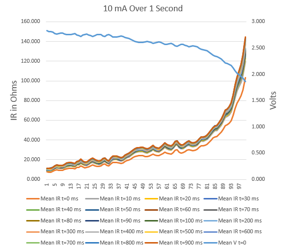
The bottom line is that the voltage the MCU sees when it first wakes up is not that which will be there mere milliseconds later. Figure on another 10% drop, on top of all of the losses detailed earlier.
May, 2015 Update: I’m told this is due to electron migration within a cell. Electrons pool on an electrode; when a load is applied these pooled charges are the first to be drawn off. It’s as if there’s a bit of capacitance involved.
12 – Watchdog Timers
Quite a few people have written asking about using watchdog timers (WDT) in battery-operated systems that achieve years-long life by snoozing 99+ percent of the time. The system may be dead to the world for hours — how does one service a WDT when the code isn’t running?
Why would you want to? How can the software crash when it’s not running?
The answer is that the code can fail while awake and accidently enter a sleep state. Running the WDT during sleep insures the system will recover.
One could wake up once a minute or so and tickle the watchdog. Generally that only requires a handful of instructions. Even when running from a 32 kHz clock (typical for ultra-low power sleep modes) the tickle will only need a ms or so of awake time. If the MCU consumes 50 uA while servicing the WDT that’s just 7.5 uAh per year of operation. Given that a CR2032 coin cell has about 220 mAh of capacity, the energy needed for managing the WDT is insignificant.
But the reality is a bit more complex. We have to work with real parts, not idealized devices.
I looked at a typical microcontroller from Microchip, picked at random from their incredibly diverse selection of “XLP” (extremely low power) devices. The PIC16LF1704/8 is a nice 8 bitter with gobs on on-board I/O, including a watchdog timer. In the low-power sleep mode the WDT consumes 14-17 uA. I started engineering when a microprocessor needed a huge honking power supply, so this is an incredibly small number. But it’s too much for long-lived coin cell operation. That compendium I referenced demonstrates that for 10 years of life from a coin cell the average current consumed can’t exceed 2.5 uA. That watchdog is unusable in this environment.
(I didn’t do an exhaustive search; possibly other MCUs from Microchip have lower-current WDTs. And I commend them for publishing these worst-case numbers; too many other vendors don’t.)
A competing MCU from TI, the MSP430F11x1a, takes only 1 to 3.4 uA in the lowest-power sleep that still has an oscillator running (to support the WDT). Nice, but 3.4 uA is far too much for these applications. The better figures assume Vdd is 2.2 volts and it’s not hot. No incremental current is listed for turning on the watchdog, which suggests that is included in these figures. However, the user’s guide reads “When the watchdog timer is not required, the WDTHOLD bit can be used to hold the WDTCNT, reducing power consumption.” That sounds like there is some, undocumented, hit for using that peripheral. Is it a nanoamp or do you have to run jumper cables to a car battery? Sans data engineers are left adrift.
Other vendors are equally vague.
Since the code can’t crash while sleeping, leave the WDT turned off during those long periods. Enable it while awake. Running, a crash will be mediated by the operating WDT. The upside of this approach is that, since the MCU is awake for such short periods, the current consumed by the WDT is insignificant and won’t drain the battery.
While awake, of course, a crash could vector to the code that disables the watchdog before going to sleep. Instead, structure the code to initialize a variable to a known value, and add offsets to it while running. That could be done in functions that are always called. Before executing the SLEEP instruction check to see if that variable contains a value that indicates the code executed correctly. Take recovery action if the variable is not correct. Or, if basically the same code runs during each awake cycle, use a timer to measure execution time; error if it deviates much from nominal.
There are other failure modes. The firmware could be perfect, but an external event — EMI or a cosmic ray impact — may scramble the MCU’s neurons. Perhaps the program counter gets altered. When the MCU wakes up it will resume operation at a random address without re-enabling the WDT. Or maybe the event flips a bit in the sleep logic so the microcontroller never wakes up.
Essentially, one would need a watchdog that operates during sleep times to counter these threats. Internal WDTs use too much current. Readers have suggested two TI parts: the TPL15111 timer (beware of footnote #4 in that datasheet), and the TPL5010.
13- Summary
This report uses the results of extensive experiments, plus analysis, to prove that most assumptions about designing ultra-low power systems are wrong. Among the most important findings:
- Sleep current is almost irrelevant
- What matters is time spent sleeping…
- … and contributions of other leaks and drains
- The internal resistance of coin cells increases hugely as the battery is discharged.
- Don’t wake up at full speed! Check the voltage as you ramp up frequency.
- Don’t use the on-board brown-out reset circuits.
- Droop will trim another 10% or so of battery capacity.
- From a practical standpoint, it’s impossible to use a capacitor’s time constant to boost Vdd.
- Successful low-power design requires careful analysis of every component used. Even poor decoupling capacitor selection will drain a battery in short order.
- I doubt anyone will get 10 years from a coin cell even with the most careful design practices.
The bottom line is to apply careful engineering judgment to all design decisions.
And test your design. You know the IR will go up as the cell’s voltage declines. Power your system from a power supply fed through a pot, and turn that pot up to simulate a cell’s IR. Run the system through sleep and wake modes, as well as brown-out-reset, to insure it will still operate correctly even as a battery approaches end of life.
source: http://www.ganssle.com/reports/ultra-low-power-design.html


x (14 Omega)")

x (0.4 Omega)")